- 您现在的位置:买卖IC网 > Sheet目录1994 > DS3232MZ+ (Maxim Integrated Products)IC RTC W/SRAM I2C 8SOIC
DS3232M
±5ppm, I2C Real-Time Clock with SRAM
19
Maxim Integrated
Test Register (13h)
SRAM (14h–FFh)
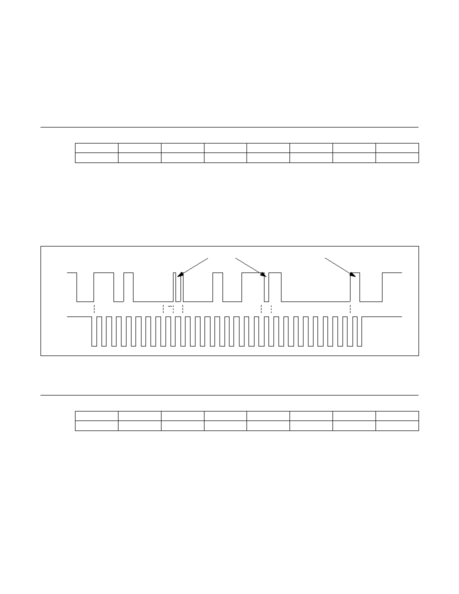
Figure 8. Software Reset I/O Execution
BIT 7
BIT 6
BIT 5
BIT 4
BIT 3
BIT 2
BIT 1
BIT 0
NAME:
SWRST
0
POR*:
0
*POR is defined as the first application of power to the device, either VBAT or VCC.
This register is used for factory test. Bits 6:0 are locked and always read as zeros. Writing to bit locations 6:0 has no affect on the
device. If the SWRST bit is set to Logic 1, the device immediately resets all internal logic and registers (except the SRAM) to their
factory-default POR state.
The device reset occurs during the normal acknowledge time slot following the receipt of the data byte carrying that SWRST
instruction; a NACK occurs due to the resetting action (see Figure 8). The I/O master should terminate the I/O string with a nor-
mal STOP instruction (on the 28th SCL clock). The SWRST bit is automatically cleared to logic 0.
BIT 7
BIT 6
BIT 5
BIT 4
BIT 3
BIT 2
BIT 1
BIT 0
NAME:
D7
D6
D5
D4
D3
D2
D1
D0
POR*:
X
*POR is defined as the first application of power to the device, either VBAT or VCC.
SDA
11
0
000
00
0000
00
0
1
SCL
SLAVE ADDRESS
REGISTER ADDRESS
SLAVE ACKs
NACK DURING SWRST
DATA
R/W
发布紧急采购,3分钟左右您将得到回复。
相关PDF资料
DS3232SN#T&R
IC RTC W/TCXO 20-SOIC
DS3234S#
IC RTC W/TCXO 20-SOIC
DS32C35-33#T&R
IC RTC ACCURATE I2C 3.3V 20-SOIC
DS3911T+
IC DAC 10BIT I2C QUAD 14TDFN
DS4000KI/WBGA
IC OSC TCXO 19.44MHZ 24-BGA
DS4026S+WCN
IC OSC TCXO 25MHZ 16-SOIC
DS4100HW+
IC OSC CLOCK 100MHZ 10LCCC
DS4266P+
IC OSC CLOCK 266MHZ 10-LCCC
相关代理商/技术参数
DS3232MZ+TRL
功能描述:实时时钟 RTC/TCMO/MEMS RoHS:否 制造商:Microchip Technology 功能:Clock, Calendar. Alarm RTC 总线接口:I2C 日期格式:DW:DM:M:Y 时间格式:HH:MM:SS RTC 存储容量:64 B 电源电压-最大:5.5 V 电源电压-最小:1.8 V 最大工作温度:+ 85 C 最小工作温度: 安装风格:Through Hole 封装 / 箱体:PDIP-8 封装:Tube
DS3232N
制造商:MAXIM 制造商全称:Maxim Integrated Products 功能描述:Extremely Accurate I2C RTC with Integrated Crystal and SRAM
DS3232S
制造商:Maxim Integrated Products 功能描述:Extremely Accurate I2C RTC
DS3232S-
制造商:MAXIM 制造商全称:Maxim Integrated Products 功能描述:Extremely Accurate I2C RTC with Integrated Crystal and SRAM
DS3232S#
功能描述:实时时钟 Integrated RTC/TCXO/Crystal RoHS:否 制造商:Microchip Technology 功能:Clock, Calendar. Alarm RTC 总线接口:I2C 日期格式:DW:DM:M:Y 时间格式:HH:MM:SS RTC 存储容量:64 B 电源电压-最大:5.5 V 电源电压-最小:1.8 V 最大工作温度:+ 85 C 最小工作温度: 安装风格:Through Hole 封装 / 箱体:PDIP-8 封装:Tube
DS3232S#T&R
制造商:Maxim Integrated Products 功能描述:EXTREMELY ACCURATE I2C RTC 20SOIC W - Tape and Reel 制造商:Maxim Integrated Products 功能描述:DS3232 3V 20P SOIC 制造商:Maxim Integrated Products 功能描述:IC RTC W/TCXO 20-SOIC
DS3232S#T&R
功能描述:实时时钟 Integrated RTC/TCXO/Crystal RoHS:否 制造商:Microchip Technology 功能:Clock, Calendar. Alarm RTC 总线接口:I2C 日期格式:DW:DM:M:Y 时间格式:HH:MM:SS RTC 存储容量:64 B 电源电压-最大:5.5 V 电源电压-最小:1.8 V 最大工作温度:+ 85 C 最小工作温度: 安装风格:Through Hole 封装 / 箱体:PDIP-8 封装:Tube
DS3232SN
制造商:Maxim Integrated Products 功能描述:Extremely Accurate I2C RTC